Balbharti Maharashtra State Board 12th Physics Important Questions Chapter 16 Semiconductor Devices Important Questions and Answers.
Maharashtra State Board 12th Physics Important Questions Chapter 16 Semiconductor Devices
Question 1.
What is a PN-junction diode? What is a depletion region? What is barrier potential in a PN-junction?
Answer:
PN-junction diode: A two-terminal semiconductor device consisting of a PN-junction is called a PN- junction diode.
Depletion region: The neighbourhood of the junction between a p-type layer and an n-type layer within a single semiconducting crystal is depleted of free (or mobile) charge carriers. This is called the depletion region or depletion layer.
Barrier potential: The electric potential difference across the PN-junction is called the potential barrier or barrier potential.
[Note: Under the open-circuit condition (no applied potential difference), the width of the depletion region and the height of the potential barrier have their equilibrium values. The width of the depletion region in an unbiased pn-junction diode ranges from 0.5 pm to 1 pm and depends on the dopant concentrations. The barrier potential is about 0.3 V for Ge junction diode and about 0.7 V for Si junction diode.]
Question 2.
Explain the forward bias and reverse bias conditions of a diode.
Answer:
Forward-biased state : When the positive terminal of a cell is connected to the p side of the junction and the negative terminal to the n side, the diode is said to be forward biased. When forward biased, the depletion region narrows and, consequently, the potential barrier is lowered. This causes the majority charge carriers of each region to cross into the other region. This way the diode conducts when forward biased; the total current across the junction is called the forward current and is due to both electron and hole currents. Because of the narrowing of the depletion region, a forward-biased junction diode has a very low resistance and acts as a closed switch.
Reverse-biased state : A pn-junction diode is said to be reverse biased when the positive terminal of a cell or battery is connected to the n side of the junction, and the negative terminal to the p side. When reverse biased, the depletion region widens and the potential barrier is increased, the majority charge carrier concentration in each region decreases against the equilibrium values and the reverse-biased junction diode has a high resistance. The diffusion current across the junction becomes zero. Thus, the diode does not conduct when reverse biased and is said to be in a quiescent or non-conducting state, i.e., it acts as an open switch (almost).
![]()
Question 3.
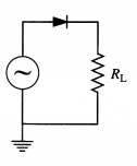
What is rectification? What is a rectifier? How does a pn-junction diode act as a rectifier?
Answer:
- The process of converting an alternating voltage (or current) to a direct voltage (or current) is called rectification.
A circuit or device that is used to convert an alternating voltage (or current) to a direct voltage (or current) is called a rectifier. A rectifier produces a unidirectional but pulsating voltage from an alternating voltage. - When an alternating voltage is applied across a pn-junction diode, the diode is forward-biased and reverse-biased during alternate half cycles.
- During the half cycle when the diode is forward- – biased, it conducts. Therefore, there is a current through it from the p-region to the n-region.
- During the next half cycle, it is reverse-biased and does not conduct. Therefore, current passes only in one direction through the circuit. This way, a pn-junction diode acts as a rectifier.
Question 4.
Explain the need for rectification/rectifiers.
Answer:
Nowadays electrical energy is generated, transmitted and distributed in the form of alternating voltage because it is simpler and more economical than direct current transmission and distribution. Another important reason for the widespread use of alternating voltage in preference to direct voltage is the fact that alternating voltage can be conveniently changed in magnitude by means of a transformer.
However, most electrical and electronic systems need a dc voltage to work. Since the transmitted voltage is very high and alternating, we need to reduce the ac line voltage and then convert it to a relatively constant dc output voltage. The power-line voltage is sequentially stepped down at the distribution substations. At the consumer end, the ac voltage is rectified using junction diodes to dc voltage.
Question 5.
Draw a neat block diagram of a dc power supply and state the function of each part.
OR
With the help of a block diagram, explain the scheme of a power supply for obtaining dc output voltage from ac line voltage.
Answer:
A consumer electronic system called a dc power supply produces a fairly constant dc voltage from ac supply voltage. Below figure shows a functional block diagram of the circuits within a power supply.
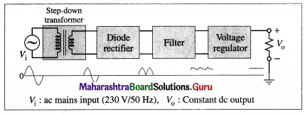
Block diagram of dc power supply with waveforms at each stage
The ac supply voltage is usually stepped-down by a transformer and its secondary voltage is converted to a pulsating dc by a diode rectifier. By the superposition theorem, this rectifier output can be looked upon as having two different components : a dc voltage (the average value) and an ac voltage (the fluctuating part). The filter circuit smooths out the pulsating dc. It blocks almost all of the ac component and almost all of the dc component is passed on to the load resistor. Figure shows the filtered output for a rectified full-wave dc. The only deviation from a perfect dc voltage is the small ac load voltage called ripple. A well-designed filter circuit minimizes the ripple. In this way, we get an almost perfect dc voltage, one that is almost constant, like the voltage out of a battery.
The regulation of a power supply is its ability to hold the output steady under conditions of changing input or changing load. As power supplies are loaded, the output voltage tends to drop to a lower value. Nowadays, an integrated circuit (IC) voltage regulator is connected between a filter and the load resistor, especially in low-voltage power supplies. This device not only reduces the ripple, it also holds the output voltage constant under varying load and ac input voltage.
![]()
Question 6.
Distinguish between a half-wave rectifier and full-wave rectifier.
Answer:
| Half-wave rectifier | Full-wave rectifier |
| 1. A device or a circuit which rectifies only one-half of each cycle of an alternating voltage is called a half-wave rectifier. | 1. A device or a circuit which rectifies both halves of each cycle of an alternating voltage is called a full-wave rectifier. |
| 2. A half-wave rectifier circuit uses a single diode which conducts for only one-half of each cycle. | 2. A full-wave rectifier circuit uses at least two diodes which conduct alternately for consecutive halves of each cycle. |
Question 7.
State any two advantages of a full-wave rectifier.
Answer:
- A full-wave rectifier rectifies both halves of each cycle of the ac input.
- Efficiency of a full-wave rectifier is twice that of a half-wave rectifier.
- The ripple in a full-wave rectifier is less than that in a half-wave rectifier.
Ripple factors for a full-wave and half-wave rectifiers are respectively, 0.482 and 1.21.
Question 8.
Explain ripple in the output of a rectifier. What is ripple factor?
Answer:
The output of a rectifier is a pulsating dc. By the superposition theorem, this rectifier output can be looked upon as having two different components : a dc and an ac. The direct current is the average value of the pulsating current, averaged over each half cycle of the ac input. The ac component in the output is called the ripple. Ripple is undesirable in most electronic circuits and devices.
The ratio of the root-mean-square value of the ac component to the average value of the dc component in the filtered rectifier output is known as the ripple factor.
Ripple factor = \(\frac{(r m s \text { value of ac component })}{\text { (average value of dc component) }}\)
Percentage ripple = ripple factor × 100%
This factor mainly decides the effectiveness of a filter circuit in a power supply, i.e., smaller the value of this factor, lesser is the ac component in comparison to the dc component. Hence, more effective is the filter.
![]()
Question 10.
Explain the action of a capacitive filter with necessary diagrams.
Answer:
Consider a simple capacitive filter added to a full-wave rectifier circuit, Fig. 16.6(a). A capacitor is a charge storage device that it can deliver later to a load.
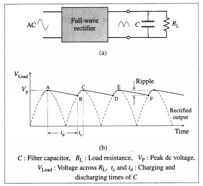
(a) Capacitive filter at the output of a full-wave rectifier (b) Waveform of filtered output
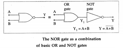
In the first quarter cycle, the capacitor charges as the rectifier output peaks. Later, as the rectifier output drops off during the second quarter cycle, the capacitor discharges and delivers the load current. The voltage across the capacitor, and the load, decreases up to a point B when the next voltage peak recharges the capacitor again. To be effective, a filter capacitor should be only slightly discharged between peaks. This will mean a small voltage change across the load and, thus, small ripple. As shown in Fig. (b), the capacitor supplies all the load current from A to B; from B to C, the rectifier supplies the current to the load and the capacitor.
The discharging time constant of a filter capacitor has to be long as compared to the time between the voltage peaks. For the same capacitor used with a half-wave rectifier, the capacitor will have twice the time to discharge, and the ripple will be greater. Thus, full-wave rectifiers are used when a low ripple factor is desired.
Question 11.
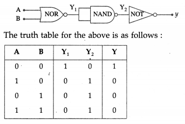
What is regulation in a dc power supply ? OR Explain unregulated power supply and regulated power supply.
Answer:
Voltage regulation is am important factor of a power supply. Regulation is its ability to hold the dc output steady under conditions of changing ac input or changing load. The output voltage under no-load condition (no current drawn from the supply) tends to drop to a lower value when load current is drawn from the supply (under load). The amount the dc voltage changes between the no-load and full-load conditions is described by a factor called voltage regulation.
Voltage regulation = \(\frac{\text { no-load voltage }-\text { full-load voltage }}{\text { full-load voltage }}\)
Question 12.
What is a regulated power supply?
Answer:
A dc power supply whose preset output voltage remains constant irrespective of variations in the line voltage or load current is called a regulated power supply.
Question 13.
What is a unregulated power supply ?
Answer:
A dc power supply whose output changes when a load is connected across it is called unregulated power supply.
Question 14.
Name any four common special-purpose diodes.
Answer:
Special-purpose diodes :
- Zener diode
- light emitting diode (LED)
- photodiode
- solar cell.
Question 15.
What is meant by breakdown of a pn-junction? Name two important mechanisms of junction breakdown.
Answer:
In a reverse-biased pn-junction, the depletion region is wider and the potential barrier is higher over equilibrium values. The majority charge carrier concentration in each region decreases from the equilibrium values and the diffusion current across the junction is zero. Only a very very small current flows due to the motion of minority charge carriers. Thus, the principal characteristic of a pn-junction diode is that it rectifies, i.e., it conducts significantly in one direction only.
When a sufficiently large reverse voltage is applied to a pn-junction, there is an abrupt strong increase in the reverse current and its rectifying properties are lost. This is known as junction breakdown. The absolute value VB of the voltage at which the phenomenon occurs is called breakdown voltage. The breakdown process is not inherently destructive and is reversible.
Two important breakdown mechanisms are the Zener breakdown (due to tunneling effect) and avalanche breakdown (due to avalanche multipli-cation).
![]()
Question 16.
Explain Zener breakdown.
Answer:
In a reverse-biased pn-junction, the depletion region is wider and the potential barrier is higher over equilibrium values. The electric field in the depletion region is from the n- to the p-region. When a sufficiently large reverse voltage is applied to a pn-junction, the junction breaks down and conducts a very large current. Of the two important breakdown mechanisms, Zener breakdown takes place in heavily doped diodes.
Usually, the energy that an electron can gain from even a strong field is very small. However, the depletion region is very narrow in a heavily doped diode. Because of this, the electric field across the depletion region is intense enough to break the covalent bonds between neighbouring silicon atoms and pull electrons out of their orbits. This results in conduction electrons and holes. In the energy band diagram representation, this corresponds to the transition of an electron from the valence band to the conduction band and become available for conduction.
The current increases with increase in applied voltage, but without further increase in voltage across the diode. This process, in which an electron of energy less than the barrier height penetrates through the energy bandgap, is called tunneling (a quantum mechanical effect). The creation of electrons in the conduction band and holes in the valence band by tunneling effect in a reverse- biased pn-junction diode is called the Zener effect.
[Notes : (1) Tunneling occurs only if the electric field is very high. The typical field for silicon and gallium arsenide is > 106 V / cm. To achieve such a high field, the doping concentrations for both p- and w-regions must be quite high (>1018 cm-3). (2) Zener breakdown or Zener effect is named in honour of Clarence M. Zener (1905-93), US physicist, who explained the breakdown mechanism. (3) Avalanche breakdown occurs in diodes with a doping concentration of ≅ 1017 cm-3 or less. The carriers gain enough kinetic energy to generate electron-hole pairs by the avalanche process when the value of reverse | V | becomes large. An electron in the conduction band can gain kinetic energy before it collides with a valence electron. The high-energy electron in the conduction band can transfer some of its kinetic energy to the valence electron to make an upward transition to the conduction band. An electron-hole pair is generated. All such electrons and holes accelerate in the high field of the depletion region and, in turn, generate other electron-hole pairs in a like manner. This process is called the avalanche process.]
Question 17. What is a Zener diode?
Answer:
A Zener diode is a heavily doped pn-junction diode operated in its breakdown region. Zener breakdown occurs when the breakdown voltage is less than about 6 V while avalanche breakdown occurs in lightly doped diodes and for breakdown voltage greater than 6 V. However, the Zener effect was discovered before the avalanche effect, so all diodes used in the breakdown region came to be known as Zener diodes.
Question 18.
Explain the use of a resistor in series with a Zener diode.
Answer:
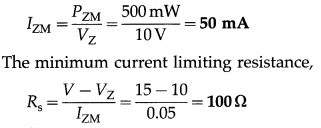
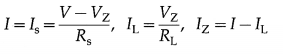
The I-V characteristics in the breakdown region of a Zener diode is almost vertical. That is, the current IZ can rapidly increase at constant VZ. To prevent damage due to excessive heating, the Zener current should not exceed the rated maximum current, IZM. Hence, a current-limiting resistor Rs is connected in series with the diode.
IZ and the power dissipated in the Zener diode will be large for IL = 0 (no-load condition) or when IL is less than the rated maximum (when Rs is small and RL is large). The current-limiting resistor Rs is so chosen that the Zener current does not exceed the rated maximum reverse current, IZM when there is no load or when the load is very high.
The rated maximum power of a Zener diode is
PZM = IZM = VZ
At no-load condition, the current through Rs is Z = IZM and the voltage drop across it is V – VZ, where V is the unregulated source voltage. The diode current will be maximum when V is maxi-mum at Vmax and I = IZM. Then, the minimum value of the series resistance should be
Rs, min = \(\frac{V_{\max }-V_{Z}}{I_{Z M}}\)
A Zener diode is operated in the breakdown region. There is a minimum Zener current, IZ(min), that places the desired operating point in the breakdown region. There is a maximum Zener current, IZM, at which the power dissipation drives the junction temperature to the maximum allowed. Beyond that current the diode can be damaged. Hence, the supply voltage must be greater than Vz and the current-limiting resistor must limit the diode current to less than the rated maximum, IZM.
![]()
Question 19.
State any two applications of a Zener diode.
Answer:
Applications of a Zener diode :
- Voltage regulator
- Fixed reference voltage in biasing transistors
- Peak clipper in a wave shaping circuit
- Meter protection from voltage fluctuations.
Question 20.
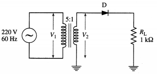
Solve the following :
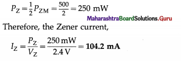
(1) A Zener diode has a Zener voltage of 2.4 V and a 500 mW power rating. What should be the maxi-mum current through the diode if you design conservatively with a safety factor of 2?
Solution:
Data : Vz = 2.4 V, PZM = 500 mW A conservative design includes a safety factor to keep the power dissipation well below the rated maximum power. Thus, with a safety factor of 2, the operating power of the Zener diode is
(2) A 10 V regulated power supply uses a Zener diode of 500 mW power rating with an input voltage of 15 V dc and a current limiting resistor of 500 Ω. If a load of 1 kΩ is connected across the diode, is the diode in the breakdown region?
Solution:
Data: V = 15V, VZ = 10V, Rs = 500 Ω, RL =1000 Ω
The supply current,
∴ The diode current, IZ = I – IL = 0
Thus, the Zener diode is at the threshold of break down and there will not be any regulation.
(3) A 10 V regulated power supply is designed using a Zener diode of 500 mW power rating with an input voltage of 15 V dc. A load of 1 kΩ is to be connected across the diode. Calculate (a) the rated maximum current through the diode (b) the mini mum value of the series resistance.
Solution:
Data: V = 15V, VZ = 10 V, PZM = 500 mW,
RL = 1000 Ω, Rs = 200 Ω
The rated maximum Zener current,
![]()
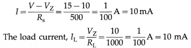
(4) In the above problem, calculate the load current. If a series resistance of 200 Ω is used, what is the Zener current ?
Solution:
Data : V = 15 V, VZ = 10 V, PZM = 500 mW, RL = 1000 Ω, Rs = 200 Ω
The current through Rs is
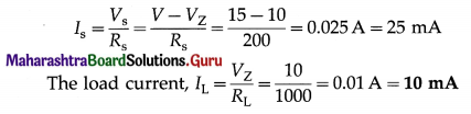
∴ The zener current,
IZ = Is – IL = 25 – 10 = 15 mA
(5) A Zener regulator has an input voltage that may vary from 15 V to 20 V while the load current may vary from 5 mA to 20 mA. If the Zener voltage is 12 V, calculate the maximum series resistance.
Solution:
Data : Vlow = 15 V, Vhigh = 20 V, VZ = 12 V,
IL, min = 5mA, IL, max = 20mA
Question 21.
What is a photodiode?
Answer:
A photodiode is a special purpose reverse-biased pn-junction diode that generates charge carriers in response to photons and high energy particles, and passes a photocurrent in the external circuit proportional to the intensity of the incident radiation. The term photodiode usually means a sensor that accurately detects changes in light level. Hence, it is sometimes called a photodetector or photosensor which operates as a photoelectric converter.
Question 22.
Explain the I-V characteristics of a photodiode.
Answer:
When a Si photodiode is operated in the dark (zero illumination), the current versus voltage characteristics observed are similar to the curve of a rectifier diode as shown by curve (1) in figure. This dark current in Si photodiodes range from 5 pA to 10 nA.
When light is incident on the photodiode, the curve shifts to (2) and increasing the incident illuminance (light level) shifts this characteristic curve still further to (3) in parallel. The magnitude of the reverse voltage has nearly no influence on the photocurrent and only a weak influence on the dark current. The normal reverse currents are in tens to hundreds of microampere range.
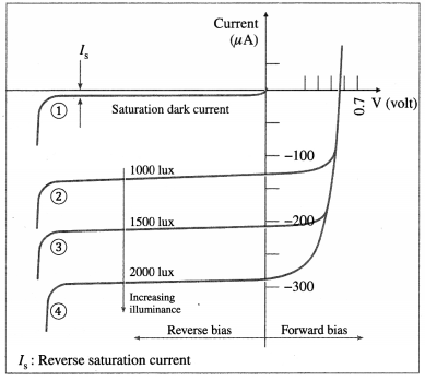
The I-V characteristics of a photodiode showing dark current and photocurrent for increasing illuminance
The almost equal spacing between the curves for the same increment in luminous flux reveals that the reverse current and luminous flux are almost linearly related. The photocurrent of the Si photo-diode is extremely linear with respect to the il-luminance. Since the total reverse current is the sum of the photocurrent and the dark current, the sensitivity of a photodiode is increased by minimizing the dark current.
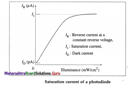
Question 23.
Explain saturation current of a photodiode with a neat labelled diagram.
Answer:
When a reverse-biased photodiode is illuminated, the reverse current at a constant reverse voltage is directly proportional to the illuminance. The de-pendence of the photocurrent on the illuminance is very linear over six or more orders of illuminance, e.g., in the range from a few nanowatts to tens of milliwatts with an active area of a few mm2. But after a certain value of reverse current, the current does not increase further with increasing light intensity. This constant value is called the satura-tion current of the photodiode.
Question 24.
What is (i) dark current (ii) dark resistance of a photodiode?
Answer:
(i) Dark current: The current associated with a photo-diode with an applied reverse bias during operation in the dark (zero illumination) due to background radiation and thermally excited minority saturation current. It is of the order of picoamperes to nanoamperes. Larger active areas or increase in temperature and reverse bias result in higher dark current.
(ii) Dark resistance : The ratio of maximum withstandable reverse voltage to the dark current of a photo-diode is called dark resistance of that diode.
Dark resistance, Rd = \(\frac{\text { (maximum reverse voltage) }}{(\text { dark current })}\)
![]()
Question 25.
State any four advantages of a photodiode.
Answer:
Advantages of a photodiode :
- Quick response to light.
- High operational speed.
- Excellent linear response over a wide dynamic range.
- Low cost.
- Wide spectral response.
- Compact, lightweight, mechanically rugged and long life.
Question 26.
State any two disadvantages of a photodiode.
Answer:
Disadvantages of a photodiode :
- Poor temperature stability : Reverse current is temperature dependent.
- Reverse current for low illumination is small and requires amplification.
Question 27.
State any two applications of photodiodes.
Answer:
Applications of photodiodes :
- A reverse-biased photodiode conducts only when illuminated, assuming that the dark current is essentially zero. Due to its quick response to radi-ation and high operational speed, photodiodes are used in high-speed counting or switching applications.
- Extensively used in an fibreoptic communication system.
- As photosensors/photodetectors for detection of UV radiations and accurate measurement of illumination. Avalanche photodiodes have increased responsivity and can be used as photomultipliers, especially for low illumination.
- In burglar alarm systems as normally closed switch until exposure to radiation is interrupted. When interrupted, the reverse current drops to the dark current level and sounds the alarm.
- In an optocoupler, a photodiode is combined with a light-emitting diode to couple an input signal to the output circuit. The key advantage of an optocoupler is the electrical isolation between the input and output circuits, especially in high voltage applications. With an optocoupler, the only contact between the input and the output is a beam of light.
Question 28.
Name two types of solar energy devices.
Answer:
Two major types of devices converting solar energy in usable form are
- photothermal devices, which convert the solar energy into heat energy
- photovoltaic devices, which convert solar energy into electrical energy.
![]()
Question 29.
What is a solar cell ? State the principle of its working.
Answer:
A solar cell is an unbiased pn-junction that converts the energy of sunlight directly into electricity with a high conversion efficiency.
Principle : A solar cell works on the photovoltaic effect in which an emf is produced between the two layers of a pn-junction as a result of irradiation.
Question 30.
Describe the output characteristics of a solar cell with a neat labelled graph.
Answer:
Output characteristic of a solar cell : The output characteristic, I-V curve, of a solar cell exposed to sunlight is plotted by varying the load resistance (Rr) from zero to infinity and measuring the corresponding current and voltage.
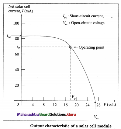
The short-circuit condition occurs when RL = 0 so that V = 0. The current in this case is referred to as the short-circuit current ISC. The open-circuit condition occurs when RL = ∞. The net current in this case is zero and the voltage produced is called as the open-circuit voltage VOC. Increasing the lightsensing area or light intensity per single solar cell produces a proportionate increase in ISC. VOC is independent of these parameters.
The operating point of a solar cell module is the point (Vp, Ip) on the I-V curve which delivers maximum power to the load. For this, Vp/ Ip must be equal to RL.
[Note : The photocurrent in a solar cell is always in the reverse-bias direction so that the I-V graph is in the fourth quadrant.]
Question 31.
State the material selection criteria for solar cells.
Answer:
Criteria for materials to be used in solar cells :
- Band gap energy must be between 1 eV and 1.8 eV. (The best band gap of a solar cell is in the region of 1.5 eV.)
- It must have high optical absorption.
- It must have high electrical conductivity.
- The raw material must be available in abundance and the cost of the material must be low.
Question 32.
Name the common materials for solar cells.
Answer:
Optimized band gap for solar cells is close to 1.5 eV. Some of the common materials for solar cells are
- silicon (Si), EG = 1.12 eV – currently the most popular material but has low absorption coefficient and high temperature dependence,
- gallium arsenide (GaAs), EG = 1.42 eV -by far the most widely used, especially for high end applications like satellites. Its absorption coefficient is about ten times better than silicon and doesn’t have the same temperature dependence.
- copper-indium diselenide (CIS), EG = 1.01 eV – has the highest optical absorption, but gallium is introduced in the lattice to raise the band gap energy closer to the solar ideal. This resulted in the popular copper-indium-gallium diselenide (Culn- GaSe2 or CIGS) material for photovoltaic cell. By variation of Ga fraction, a band gap of around 1.48 eV has been achieved.
- cadmium telluride (CdTe), EG = 1.44 eV-made from the II-VI group elements.
![]()
[Notes : (1) By far the most widely used III-V solar cell is gallium arsenide (GaAs). Other III-V semiconductors-indium phosphide (InP), gallium antimonide (GaSb), aluminium gallium arsenide (AlGaAs), indium gallium phosphide (InGaP), and indium gallium arsenide (InGaAs)-exchange group III elements to make different band gap energies. III-V semiconductors offer a great host of advantages over silicon as a material for photovoltaics. However, the biggest drawback is cost. (2) The theoretical limit on the thermodynamic efficiency of single-junction solar cells is ~ 30%. Hence, today’s most efficient technology for the generation of electricity from solar radiation is the use of multi-junction solar cells made of III-V compound semiconductors. Efficiencies up to 39% have al-ready been reported under concentrated sunlight. These solar cells have initially been developed for powering satellites in space and are now starting to explore the terrestrial energy market through the use of photovoltaic concentrator systems. A triple-junction solar cell, Ga0.35In0.65P/Ga0.83In0.17As/Ge, has been demonstrated by a conversion efficiency of 41.1% at 454 kW/m2]
Question 33.
State any four uses of solar cells.
Answer:
Uses of solar cells :
- A solar cell array consisting of a set of solar cells is used during daylight hours to power an electrical equipment as well as to recharge batteries which can then be used during night.
- Solar cell arrays provide electrical power to equipment on a satellite as well as at remote places on the Earth where electric power lines are absent.
- Large-scale solar power generation systems linked with commercial power grid.
- Independent power supply systems for radar detectors, monitoring systems, radio relay stations, roadlights and roadsigns.
- Indoor uses include consumer products like, calculators, clocks, digital thermometers, etc. (They use very low levels of power and work under lowbrightness long-wavelength light from incandescent lamps, etc.)
Question 34.
What is a light-emitting diode (LED) ?
Answer:
A light-emitting diode (LED) is a forward-biased pn-junction diode formed from compound semiconductor materials such as gallium arsenide (GaAs) in which light emission can take place from direct radiative recombination of excess electron-hole pairs. A photon is emitted when an electron in the conduction band recombines with a hole in the valence band.
In infrared emitting LEDs, the encapsulating plastic lens may be impregnated or coated with phosphorus. Then, phosphorescence of the phos-phorus gives off visible light.
[Note: In an ordinary pn-junction diode, energy released in electron-hole recombination process is absorbed in the crystal structure as heat.]
Question 35.
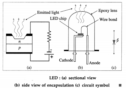
Describe with a neat diagram the construction of an LED.
Answer:
Construction : A light-emitting diode is a forward- biased pn-junction diode formed from compound semiconductor materials. As shown in Fig. 16.14(a), the top metal contact to the n-layer (say) is provided with a window for the emitted light to escape. The diode chip is encapsulated in a transparent plastic lens. The cathode and anode leads from the metal contacts to the n-and p-layers, respectively, are provided for external connections, shown in figure.
The negative electrode (cathode) is identified by a notch or flat spot on the plastic body, or the cathode lead is shorter than the anode.
![]()
Question 36.
Draw the I-V forward characteristics of an LED and explain it.
Answer:
Explanation : The forward characteristic of an LED is similar to an ordinary junction diode. The diode starts conducting only after the forward-bias voltage overcomes the barrier potential. Thereafter the current increases exponentially beyond the knee region.
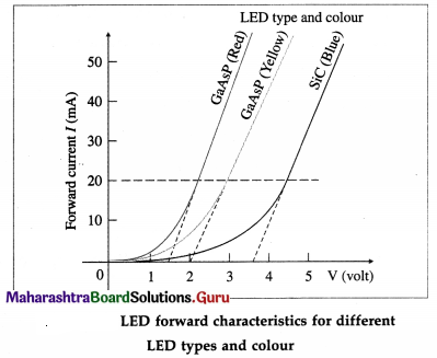
The threshold voltage is about 1.2 V for a standard red LED to about 3.6 V for a blue LED. However, these values depend on the manufacturer because of the different dopant concentrations used for the different wavelength ranges.
The intensity of the emitted light is directly propotional to the forward current. An LED is operated with a typical forward current of 20 mA- about 5 mA for a simple LED indicator to about 30 mA where a high intensity of light is needed. The LED forward current must be limited to a specified safe value using a series resistance.
The peak inverse voltage (PIV) or breakdown voltage of an LED is low, typically 5 V.
Question 37.
State any four advantages of an LED over common light sources.
Answer:
Advantages of an LED as a light source over common light sources :
- Energy efficiency : An LED is small in size, requires low operating voltage and power and is extremely energy efficient, consuming up to 90% less power than incandescent bulbs. LED’s are now capable of outputting 135 lumens/watt.
- Life and ruggedness : Being a solid state device, an LED is more rugged than bulbs with filament and has a typical life of 50000 hours or more.
- Fast switching : An LED is very fast, i.e., its switching (on / off) time is less than 1 ns.
- Brightness and colour control: The intensity of the emitted light can be varied continuously. The colour of the emitted light also can be controlled.
- Small size : Because of their small size, they can be used to produce self-luminous, static or running, seven-segment alphanumeric displays.
- Environmentally friendly : An LED being a semi-conductor device, does not contain hazardous substances like mercury (as in sodium and mercury vapour lamps).
- Operationally cheap : Since LEDs use only a fraction of the energy of an incandescent light bulb there is a dramatic decrease in power costs.
Question 38.
State any four disadvantages of an LED.
Answer:
Disadvantages of an LED light source :
(1) Blue light hazard : There is a photobiological con-cern that bright blue LEDs and cool-white LEDs are capable of exceeding safe limits.
(2) Light quality : Most cool-white LEDs have spectral output significantly different from the Sun or an incandescent bulb-peak output being at 460 nm rather than peak retinal sensitivity of 550 nm. This can cause the colour of objects to be perceived differently under cool-white LED illumination than sunlight or incandescent bulbs.
(3) Temperature dependence : An LED luminaire can overheat in high ambient temperatures and effective cooling methods using heat sinks are essential for high-power LEDs. (Although the thermal power involved is not very large, it is released within a very small volume and area.) This is especially important for automotive, medical and military applications where the light unit must operate over a large range of temperatures and yet have a low failure rate.
(4) High initial cost: LEDs are currently more expen-sive-price per lumen-in initial capital cost, than most conventional lighting technologies.
(5) Voltage sensitivity : LEDs must be operated with the voltage above the threshold and the current below the rated maximum. This requires current- limiting resistors or current-regulated power supplies.
(6) Blue light pollution : Cool-white LEDs emit pro-portionally more blue light than conventional out-door light sources such as high-pressure sodium lamps. Due to Rayleigh scattering, these LEDs can cause more light pollution than other light sources.
![]()
Question 39.
State any four applications of LEDs.
Answer:
Applications of LEDs :
- An LED is commonly used as an On/Off indicator lamp on electrical equipment.
- LEDs are used in self-luminous seven-segment alphanumeric displays of calculators and digital clocks and meters, signages, etc.
- Because of their low power consumption, LEDs are now commonly used in traffic signals, handheld torches, LED TV sets, domestic and decorative illumination and various indicator lamps in light motor vehicles and two-wheelers.
- Under certain conditions, the essentially monochromatic light emitted by an LED is also coherent. Such diode lasers have found applications in optical fibre communications, CD players, CDROM drives, laser printers, bar code scanners, laser pointers, etc.
Question 40.
What is a junction transistor?
Answer:
A junction transistor consists of two back-to-back pn-junctions forming a sandwich structure in which a thin layer of n-type or p-type semiconductor is sandwiched between two layers of opposite type semiconductor.
The three terminals of a transistor connected to its three layers are known as the emitter (E), base (B) and collector (C). One pn-junction is between the emitter and the base while the other pn-junction is between the collector and the base.
The electric current is transported by both type of carriers, electrons and holes; for this reason the device is called a bipolar junction transistor (BJT).
There are two types of junction transistors : (i) pnp transistor (ii) npn transistor.
[Note : The point-contact transistor was invented in 1947 by US physicists John Bardeen (1908-91), Walter Brattain (1902-87) and William Shockley (1910-89). A month later Shockley invented the junction transistor.]
Question 41.
Draw the circuit symbols of (i) a pnp transistor (ii) an npn transistor.
Answer:
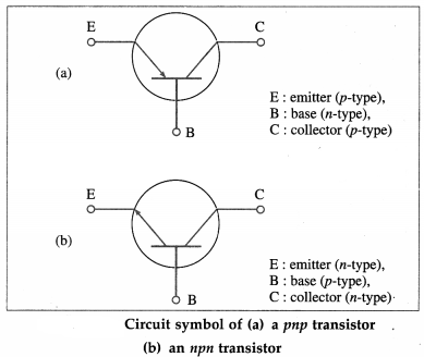
The arrow on the emitter shows the direction of current when the base-emitter junction is forward- biased. If the arrow points in (Points iN), it indicates the transistor is a pnp. On the other hand, if the arrow points out, the transistor is an npn (Not Pointing iN).
![]()
Question 42.
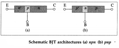
How is a junction transistor formed? Draw schematic diagrams showing the structure of the two types of BJTs.
Answer:
A bipolar junction transistor has three separately doped regions and two pn-junctions. A pnp transistor is formed by starting with a p-type substrate. An zz-type region is grown by thermally diffusing do-nor impurities into this substrate. A very heavily doped p+ region is then diffused into the n-type region. The heavily doped p + -region is called the emitter, symbol E in below figure.The narrow central n-region, with lightly doped concentration, is called the base (symbol B). The width of the base is small compared with the minority carrier diffusion length. The moderately doped p-region is called the collector (symbol C). The doping concentration in each region is assumed to be uniform.
The npn transistor is the complementary structure to the pnp transistor : A narrow p region grown into an n type substrate, by thermally diffusing acceptor impurities, forms the base. The heavily doped n + region diffused into the base forms the emitter.
Question 43.
Draw diagrams showing the two-diode analogues of npn and pnp transistors.
Answer:
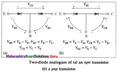
[Important note : The diode equivalents are pretty much useless except for biasing a transistor or testing with a ‘digital multimeter (DMM). The transistor action of a BJT, as explained in Question 55 is substantially different from that of two independent back-to-back pn-junctions.]
Question 46.
Explain the working of an npn transistor with a neatly labelled circuit diagram.
OR
Explain the action of a junction transistor with a neatly labelled circuit diagram.
Answer:
For normal operation of a junction transistor, the emitter-base junction is always forward biased and the collector-base junction is always reverse biased. Below figure shows the biasing of the junctions for an npn transistor connected as an amplifier with the common-base configuration, that is, the base lead is common to the input and output circuits. The emitter-base junction is forward biased by the battery VBB while the collector-base junction is reverse biased by the battery VCC. VBB should be greater than the emitter-base barrier potential (the threshold voltage). The arrows of the various currents indicate the direction of current under normal operating conditions (also called the active mode).
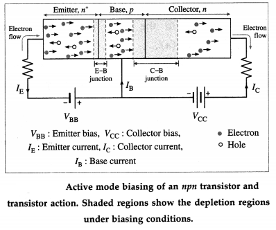
Since the emitter-base junction is forward biased, majority carriers electrons in the n+ emitter are injected into the base and holes (majority carriers in the p-type base) are injected from the base into the emitter. Under the ideal-diode condition, these two current components constitute the total emitter current IE.
The emitter is a very heavily doped n-type region. Hence, the current between emitter E and base B is almost entirely electron current from E into B across the forward-biased emitter junction.
The p-type base is narrow and the hole density in the base is very low. Therefore, virtually all the injected electrons (more than 95%) diffuse right across the base to the collector junction without recombining with holes. Since the collector junction is reverse biased, the electrons on reaching the collector junction are quickly swept by the strong electric field there into the n-type collector region, where they constitute the collector current IC.
In practice, about 1% to 5% of the holes from the emitter recombine with holes in the base layer and cause a small current IB in the base lead. Therefore,
IE = IB + IC ≈ IC
Therefore, carriers injected from a nearby emitter junction can result in a large current flow in a reverse-biased collector junction. This is the transistor action, and it can be realized only when the two junctions are physically close enough to interact as described.
If a pnp transistor is used, the battery connections must be reversed to give the correct bias. The conduction process is similar but takes place instead by migration of holes from emitter to collector. A few of these holes recombine with electrons in the base.
[Notes : (1) If, the two junctions are so far apart that all the injected electrons are recombined in the base before reaching the base-collector junction, then the transistor action is lost and the p-n-p structure becomes merely two diodes connected back to back. (2) Use of double-subscripted voltage notation in transistor circuits : same subscripts (viz., Vm and Vcc) represent the voltage of a biasing battery; different subscripts (viz, VBB and VCC) are used to indicate voltage between two points. Single subscripts (as in Fig. 16.19) are used for a node voltage, that is, the voltage between the subscripted point and ground.]
![]()
Question 47.
What are the different transistor configurations in a circuit? Show them schematically.
Answer:
There are three configurations in which a transistor may be connected in a circuit:
(a) Common-emitter (CE) : The emitter terminal is common to the input and output circuits.
(b) Common-base (CB) : The base terminal is common to the input and output circuits.
(c) Common-collector (CC) : The collector terminal is common to the input and output circuits.
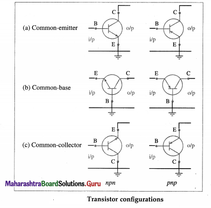
[Notes : (1) CE: Produces the highest current and power gain of all the three bipolar transistor configurations the reason why it is the most commonly used configuration for transistor based amplifiers. The emitter is grounded and the input signal applied between the base and emitter. The input impedance is small due to the forward biasing of the EB-junction. The output taken from between the collector and emitter, as well as the outputimpedance, are large due to the reverse biased CB-junction. However, its voltage gain is much lower. – (2) CB : The base terminal is grounded, the input signal is applied between the base and emitter terminals while the output signal is taken from between the base and collector terminals. Though its high frequency response is good for single stage amplifier circuits, it is not very common due to its low current gain characteristics and low input impedance. (3) CC : Very useful for impedance matching applications because of the very large ratio of input impedance to output impedance. The collector is grounded and the input signal is directly given to the base. The output is taken across the load resistor in series with the emitter. Hence, the current through the load resistor is the emitter current and the current gain of the configuration is approximately equal to the β value of the transistor.]
Question 48.
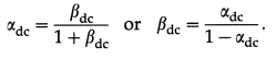
State the relation between the dc common-base current ratio (αdc) and the dc common-emitter current ratio (βdc).
Answer:
Question 49.
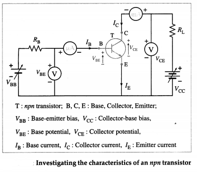
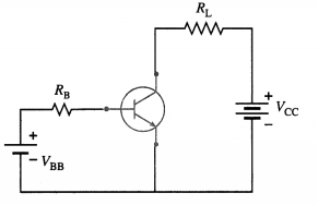
Draw a neat labelled circuit diagram to study the characteristics of a transistor in common- emitter configuration.
Answer:
![]()
Question 50.
Explain with necessary graphs (1) input (base) (2) output (collector) characteristics of a transistor in common-emitter configuration.
Answer:
Common-emitter characteristics :
(1) Input or base characteristics : This is a set of curves of base current IB against base to emitter voltage VBE for different constant collector to emitter voltages VCE shown in figure.
Keeping collector voltage VCE constant, base voltage is gradually increased from zero. Initially, IB is zero till VBE is less than the threshold voltage for the forward-biased base-emitter junction, 0.7 V for silicon and 0.3 V for germanium. For VBE greater than the threshold voltage, IB increases steeply.
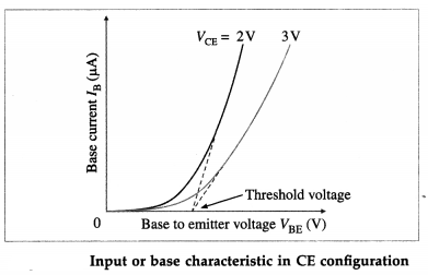
For a constant collector voltage VCE, the dynamic input resistance (ri) is defined as the ratio of the differential change in the base-to-emitter voltage (∆VBE) to the corresponding change in the base current (∆ICE).
ri = (\(\frac{\Delta V_{\mathrm{BE}}}{\Delta I_{\mathrm{B}}}\))VCE = constant
(2) Output or collector characteristics : This is a set of curves of collector current IC against collector-to- emitter voltage VCE for different constant base currents IB, shown in figure.
(i) For VBE less than the threshold voltage for the junction, IB = 0 and IC = 0, i.e., there is no current through the transistor. Both the junctions are reverse biased and the transistor acts like an open switch. Then the transistor is said to be switched Fully-OFF or in the cut-off region or OFF-mode.
(ii) The base current is set to a suitable value by varying the base-to-emitter voltage VBE to a value greater than the threshold voltage. Then, the collector-to-emitter voltage VCE is varied and the variation of IC is plotted against VCE. For very small values of VCE, ideally zero, IC is maximum, equal to VCC/ RL. Both the junctions are forward biased and the transistor acts like a closed switch. The transistor is said to be switched Fully-ON, or in the saturation region or ON-mode.
(iii) But for values of VCE above about the threshold voltage, IC is constant and VCE has relatively little effect on it. In this region, called as the active region, IC is determined almost entirely by IB. In this region, the common-emitter current gain β is large.
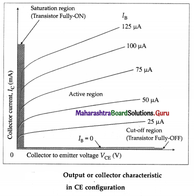
For a constant base current IB, the dynamic output resistance (r0) is defined as the ratio of the differential change in the collector-to-emitter voltage (∆VCE) to the corresponding change in the collector current (∆IC).
r0 = \(\left(\frac{\Delta V_{\mathrm{CE}}}{\Delta I_{\mathrm{C}}}\right)_{I_{\mathrm{B}}=\text { constant }}\)
Question 51.
What is an amplifier? Explain the use of a transistor as an amplifier.
OR
Draw a neat circuit diagram of a transistor CE- amplifier and explain its working.
Answer:
A device that increases the amplitude of voltage, current or power of a weak alternating signal, by drawing energy from a separate source other than the signal, is called an amplifier.
Principle : The collector current can be controlled by a small change in the base current.
Electric circuit: Consider the use of a npn transistor as an amplifier in the widely used common- emitter (CE) configuration in which the emitter is common to the input and output circuits, shown in figure. The emitter-base junction is forward biased by the battery VBB while the collector-base junction is reverse biased by the battery VCC.
The voltage Vi to be amplified, called the signal voltage, is applied between the base and the emitter.
Working : The collector characteristics shows that in the active region, the collector current Ic is determined almost entirely by the base current IB, and collector potential Vc has relatively little effect on it.
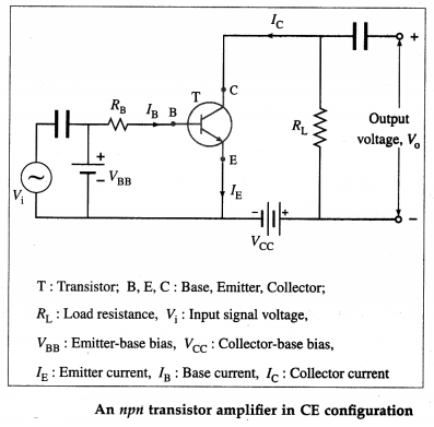
An npn transistor amplifier in CE configuration
For Vi = 0, applying Kirchhoff’s loop law to the output and input loops, we get respectively,
VCC – ICRL – VCE = 0 ……………. (1)
and PBB – IBRB – VBE = 0 …………… (2)
The applied signal voltage causes small changes ∆VBE in the emitter-base p.d. thereby producing variations ∆VBE in the base current.
∆VBE = ri∆IB …………. (3)
where ri is the dynamic input resistance.
BBB + Vi = IBRB + VBE + ∆IB(RB + ri)
∴ Vi = ∆IB(RB + ri) = ri∆IB
The variations in ∆IB cause proportionately larger variations ∆IC in the collector current because ∆IC = βac ∆IB, where the ac common-emitter current gain (βac) is always greater than 50. For normal operating voltages, βac is almost the same as βdc. From EQuestion(l), since VCC is constant,
∆VCC = ∆ICRL + ∆VCE = 0
The time-varying collector current produces a time-varying output voltage P0 across the load resistance RL.
V0 = ∆VCE = – ∆ICRL = – [βac∆IBRL
Thus, V0 > Vi, so that the circuit produces a voltage gain. The amplifier’s voltage gain (Av) is defined as the ratio of the output voltage to the input voltage.
Av = \(\frac{V_{\mathrm{o}}}{V_{\mathrm{i}}}=-\frac{\beta_{\mathrm{ac}} R_{\mathrm{L}}}{r_{\mathrm{i}}}\)
The minus sign indicates that the output voltage is 180° out of phase with the input voltage.
[ Note : Amplifiers use emitter bias by moving the resistor from the base circuit to the emitter circuit. This important change keeps the operating point of the transistor fixed and immune to changes in current gain. The base supply voltage is now applied directly to the base.]
![]()
Question 52.
Solve the following :
(1) The diagram shows a CE circuit using a silicon transistor. Calculate the (a) base current (b) collector current. [VBB = 2V, VCC = 10V, RB = 100 kΩ, RL = 1 kΩ, [βdc = 200]
Solution:
Data : VBB = 2 V, VCC = 10 V, RB = 100 kΩ, RL = 1 kΩ,
βdc = 200.
Since it is a silicon transistor, the emitter-base
barrier potential, VBE = 0.7 V.
The voltage across the base resistor is
VBB – VBE = 2 – 0.7 = 1.3 V
Therefore, the base current,
IB = \(\frac{V_{\mathrm{BB}}-V_{\mathrm{BE}}}{R_{\mathrm{B}}}=\frac{1.3}{10^{5}}\) = 1.3 × 10-5 = 13 μA
The collector current,
IC = βIB = 200 × 1.3 × 10-5 = 2.6 × 10⁻³ A = 2.6mA
(2) In the above problem, calculate the collector- emitter voltage (VCE).
Solution:
The collector-emitter voltage,
VCE = VCC – ICRL = 10 – (2.6 × 10⁻³)(103) = 2.6V
Question 53.
What is meant by an analog signal and an analog electronic circuit?
Answer:
An analog signal consists of a continuously varying voltage or current. An analog electronic circuit takes an analog signal as input and outputs a signal that varies continuously according to the input signal.
Question 54.
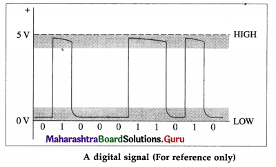
What is meant by a digital signal?
Answer:
A digital signal consists of a sequence of electrical pulses whose waveform is approximately regular, with the potential switching alternately between two values. The lower value of the potential is labelled as LOW or 0 and the higher value as HIGH or 1.
With just two bits of information, 1 or 0 (HIGH or LOW), digital circuits use binary system. A sequence of 1s and 0s is encoded to represent numerals, letters of the alphabet, punctuation marks and instructions.
[ Note : The meaning of a voltage being high or low at a particular location within a circuit can signify a number of things. For example, it may represent the on or off state of a switch or saturated transistor. It may represent one bit of a number, or whether an event has occurred, or whether some action should be taken. The high and low states can be represented as true and false statements, which are used in Boolean logic. When positive-true logic is used high = true, while high = false when negative-true logic is used.]
Question 55.
What is a digital circuit?
Answer:
An electronic circuit that processes only digital signals is called a digital circuit. There are only two voltage states present at any point within a digital circuit. These voltage states are either high or low.
The branch of electronics which deals with digital circuits is called digital electronics.
[Note : Digital circuits can store and process bits of information needed to make complex logical decisions. Digital electronics incorporate logical decision-making processes into a circuit.]
![]()
Question 56.
What are the three ways of representing a logic gate?
Answer:
A logic gate can be represented by its logic symbol, Boolean expression and the truth table.
Question 57.
How many rows are there in the truth table of a 3-input gate?
Answer:
Each of the 3 inputs can take 2 values (0 and 1).
Hence, the number of rows in the truth table of a 3-input gate = 2 × 2 × 2 = 23 = 8.
Question 58.
Name the common logic gates.
Answer:
The five common logic gates are the AND, OR, NOT, NAND and NOR gates.
Of these the AND, OR and NOT gates which respectively perform the logical AND, logical OR and logical NOT operations are called the basic logic gates. These three gates form the basis for other types of logical gates. The NAND and NOR are called the universal logic gates because any gate can be implemented by the combination of NAND and NOR gates.
Question 59.
Define the following logic gates :
(1) AND
(2) OR
(3) NOT.
Give the logic symbol, Boolean expression and truth table of each. (1 mark each )
Answer:
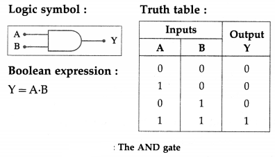
(1) The AND gate : It is a circuit with two or more inputs and one output in which the output signal is HIGH if and only if all the inputs are HIGH simultaneously.
The AND operation represents a logical multiplication.
Below figure shows the 2-input AND gate logic symbol and the Boolean expression and the truth table for the AND function.
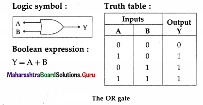
(2) The OR gate : It is a circuit with two or more inputs and one output in which the output signal is HIGH if any one or more of the inputs is HIGH.
The OR operation represents a logical addition.
Below figure shows the 2-input OR gate logic symbol, and the Boolean expression and the truth table for the OR function.
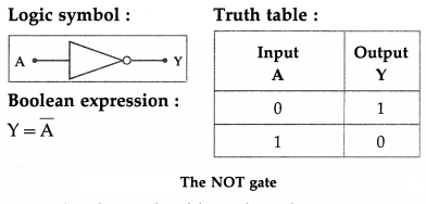
(3) The NOT gate or INVERTER : It is a circuit with one input whose output is HIGH if the input is LOW and vice versa.
The NOT operation outputs an inverted version of the input. Hence, a NOT gate is also known as an INVERTER.
The small invert bubble on the output side of the inverter logic symbol, Fig. 16.30 and the over bar (__) in the Boolean expression represent the invert function.
![]()
Question 60.
A gate generates a HIGH output when at least one of its inputs is HIGH. Which is this gate?
Answer:
It is an OR gate.
Question 61.
How will a 2-input AND gate work when both its input terminals are shorted? Give the circuit symbol and truth table.
Answer:
When both the input terminals of a 2-input AND gate are shorted, i.e., the same signal X goes to both inputs, the output is Y = X ∙ X which will give 1 if X = 1, and 0 if X = 0; hence Y = X ∙ X = X.
Circuit symbol:
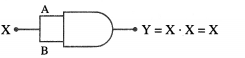
Truth table :

[Note : The OR operation gives exactly the same result. The laws Y = X ∙ X = X and Y = X + X = X are called idem potent laws.]
Question 62.
Write the Boolean expression and give the circuit symbol for a 3-input AND gate.
Answer:
Consider an AND gate with 3-inputs, A, B and C. Boolean expression : Y = A ∙ B ∙ C
Circuit symbol: ![]()
Question 63.
If only 2-input OR gates are available, draw the circuit to implement the Boolean expression Y = A + B + C.
Answer:
Implementation of Y = A + B + C using two-input OR gates :
Question 64.
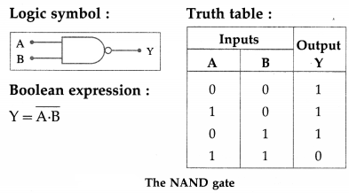
Define the logic gates (1) NAND (2) NOR.
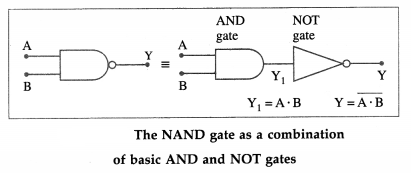
Give the logic symbol, Boolean expression and truth table of each.
How are the above gates realized from the basic gates?
Answer:
(1) The NAND gate : It is a circuit with two or more inputs and one output, whose output is HIGH if any one or more of the inputs is LOW; the output is LOW if all the inputs are HIGH.
The NAND gate is a combination of an AND gate followed by a NOT gate so that the truth table of the NAND function is obtained by inverting the outputs of the AND gate.
(2) The NOR gate: It is a circuit with two or more inputs and one output, in which the output is HIGH if and only if all the inputs are LOW.
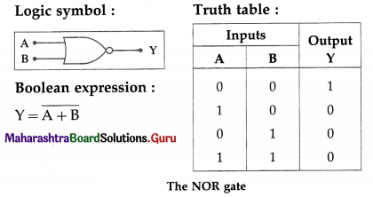
The NOR gate is realized by connecting the output of OR gate to the input of a NOT gate, so that the truth table of the NOR function is obtained by inverting the outputs of the OR gate.
![]()
Question 65.
How will a NAND gate work when all its input terminals are shorted?
Answer:
A NOT gate.
Question 66.
Define the XOR (Exclusive OR) logic gate. Give its logic symbol, Boolean expression and truth table. How is the XOR gate realized from the basic gates?
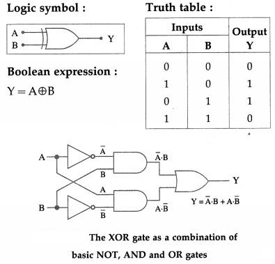
Answer:
The XOR (Exclusive OR) gate : It is a circuit with only two inputs and one output in which the output signal is HIGH if and only if the inputs are different from each other.
Question 67.
Prepare the truth tables for the following logic circuits. Write the Boolean expression for the output and name (or identify) the output function in each case.
OR
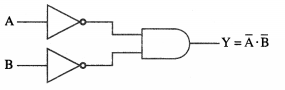
Draw the logic diagram and write the truth table for the Boolean equations
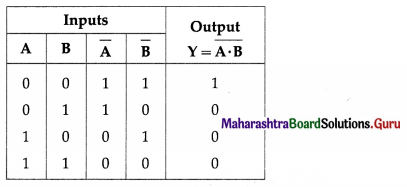
(1) Y = \(\overline{\mathrm{A}+\mathrm{B}}\)
(2) Y = \(\overline{\mathrm{A} \cdot \mathrm{B}}\)
(3) \(\overline{\mathrm{A}}+\overline{\mathrm{B}}=\overline{\mathrm{A} \cdot \mathrm{B}}\)
(4) \(\overline{\mathrm{A}} \cdot \overline{\mathrm{B}}=\overline{\mathrm{A}+\mathrm{B}}\)
Answer:
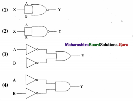
(1)
The same signal X is fed to both the inputs of the 2-input NOR gate.
The truth table shows that the output is HIGH if the input is LOW and vice versa. Therefore, the circuit functions as a NOT gate or INVERTER.
∴ Boolean expression for the output logic is Y = \(\overline{\mathrm{A}+\mathrm{B}}=\overline{\mathrm{X}}\)
(2)
The same signal X is fed to both the inputs of the 2-input NAND gate.
Truth table :
The truth table shows that the output is HIGH if the input is LOW and vice versa. Therefore, the circuit functions as a NOT gate or INVERTER.
∴ Boolean expression for the output logic is Y = \(\overline{\mathrm{A} \cdot \mathrm{B}}=\overline{\mathrm{X}}\)
(3)
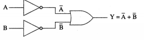
Each input of the 2-input OR gate is fed through a NOT gate, i.e., the inputs to the OR gate are \(\overline{\mathrm{A}}\) and \(\overline{\mathrm{B}}\).
Truth table:
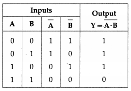
The truth table shows that the output is HIGH if any one of the inputs is LOW; the output is LOW if all the inputs are HIGH. Therefore, the circuit functions as a NAND gate.
∴ Boolean expression for the output logic is Y = latex]\overline{\mathrm{A}}+\overline{\mathrm{B}}=\overline{\mathrm{A} \cdot \mathrm{B}}[/latex]
(4)
Inverted inputs \(\overline{\mathrm{A}}\) and \(\overline{\mathrm{B}}\) are fed to the 2-input AND gate.
Truth table :
The truth table shows that the output is HIGH if and only if all the inputs are LOW. Therefore, the circuit functions as a NOR gate.
∴ Boolean expression for the output logic is Y = \(\overline{\mathrm{A}} \cdot \overline{\mathrm{B}}=\overline{\mathrm{A}+\mathrm{B}}\)
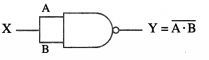
Question 68.
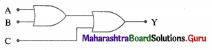
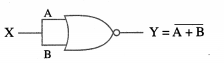
What is the equivalent logic gate for the following logic circuit?
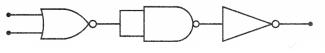
Answer:
The given logic circuit (combination of logic gates) is
i. e., the output is HIGH if and only if both the inputs are LOW, which is obtained by a NOR gate.
![]()
Question 69.
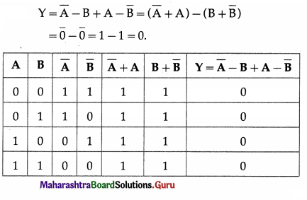
Write the truth table for the Boolean equation Y = \(\overline{\mathrm{A}}\) – B + A – \(\overline{\mathrm{B}}\).
Answer:
Multiple Choice Questions
Question 1.
An electronic circuit which converts alternating voltage into unidirectional pulsating voltage is called
(A) a transistor
(B) a rectifier
(C) an oscillator
(D) a transformer.
Answer:
(B) a rectifier
Question 2.
A pn junction exhibits rectifying property because of
(A) the potential barrier across the pn junction
(B) the difference in the doping concentrations in the p- and n-layers
(C) the avalanche breakdown when reverse biased
(D) the Zener breakdown when reverse biased.
Answer:
(A) the potential barrier across the pn junction
Question 3.
The stepped down output of a transformer, with turns ratio 5 : 1, is fed to an ideal diode D and load resistance RL. The peak load voltage is
(A) 22 V
(B) 31 V
(C) 44 V
(D) 62 V
Answer:
(D) 62 V
Question 4.
In the given circuit, the peak value of the ac source voltage is 10 V, and the diode has a negligible forward resistance and infinite reverse resistance. During the negative half cycle of the source voltage, the peak voltage across the diode is
(A) – 10 V
(B) 0
(C) 5 V
(D) 10 V
Answer:
(A) – 10 V
Question 5.
A full-wave rectifier uses a grounded centre tap on the secondary winding of a transformer and a 60 Hz source voltage across the primary winding. The output frequency of the full-wave rectifier is
(A) 30 Hz
(B) 60 Hz
(C) 120 Hz
(D) 240 Hz.
Answer:
(C) 120 Hz
Question 6.
Avalanche breakdown in a Zener diode takes place due to
(A) thermal energy
(B) light energy
(C) magnetic field
(D) accelerated minority charge carriers.
Answer:
(D) accelerated minority charge carriers.
Question 7.
A Zener diode is used as a
(A) half wave regulator
(B) half wave rectifier
(C) simple voltage regulator
(D) voltage amplifier.
Answer:
(C) simple voltage regulator
Question 8.
The current through the Zener diode in the following circuit is
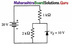
(A) 5 mA
(B) 10 mA
(C) 15 mA
(D) 30 mA.
Answer:
(A) 5 mA
Question 9.
In operation, a photodiode is
(A) unbiased
(B) always forward-biased
(C) always reverse-biased
(D) either forward-or reverse-biased.
Answer:
(C) always reverse-biased
Question 10.
The photocurrent in a photodiode is a few
(A) nanoamperes
(B) microamperes
(C) milliamperes
(D) amperes.
Answer:
(B) microamperes
Question 11.
A photodiode is used in
(A) a brake indicator
(B) an optocoupler
(C) a regulated power supply
(D) a logic gate.
Answer:
(B) an optocoupler
Question 12.
When the load resistance across a solar cell is zero, the current in the external circuit passed by the solar cell is called
(A) the open-circuit current
(B) the reverse saturation current
(C) the short-circuit current
(D) the photocurrent.
Answer:
(C) the short-circuit current
Question 13.
Which of the following is the correct circuit symbol for an LED ?
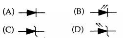
Answer:
![]()
Question 14.
The colour of light emitted by an LED depends upon
(A) its forward bias
(B) its reverse bias
(C) the band gap of the material of the semiconductor
(D) its size.
Answer:
(C) the band gap of the material of the semiconductor
Question 15.
The centre terminal of a junction transistor is called
(A) the emitter
(B) the opposite semiconductor
(C) the collector
(D) the base.
Answer:
(D) the base.
Question 16.
A transistor acts as a ‘closed switch’ when it is in
(A) the cutoff region
(B) the active region
(C) the breakdown region
(D) the saturation region.
Answer:
(D) the saturation region.
Question 17.
A junction transistor acts as
(A) a rectifier
(B) an amplifier
(C) the oscillator
(D) a voltage regulator.
Answer:
(B) an amplifier
Question 18.
When an npn junction transistor is used as an amplifier in CE-mode,
(A) the central p-type region is common to both input and output circuits
(B) the emitter terminal is common to both input and output circuits
(C) the emitter junction is reverse biased while the collector junction is forward biased
(D) the signal voltage is applied between the two n regions.
Answer:
(B) the emitter terminal is common to both input and output circuits
Question 19.
When a pnp transistor is operated in saturation region, then its
(A) the base-emitter junction is forward biased and base-collector junction is reverse biased
(B) both the base-emitter and base-collector junctions are reverse biased
(C) both the base-emitter and base-collector junctions are forward biased
(D) the base-emitter junction is reverse biased and base-collector junction is forward biased.
Answer:
(C) both the base-emitter and base-collector junctions are forward biased
Question 20.
Which logic gate corresponds to the logical equation, Y = \(\overline{\mathrm{A}+\mathrm{B}}\) ?
(A) NAND
(B) NOR
(C) AND
(D) OR
Answer:
(B) NOR
Question 21.
The output of a NAND gate is HIGH if
(A) any one or more of the inputs is LOW
(B) all the inputs are HIGH
(C) only all the inputs are simultaneously LOW
(D) only if an inverter is connected at its output.
Answer:
(A) any one or more of the inputs is LOW
Question 22.
The output of NOR gate is HIGH, when
(A) all inputs are HIGH
(B) all inputs are LOW
(C) only one of its inputs is HIGH
(D) only one of its inputs is LOW.
Answer:
(B) all inputs are LOW
Question 23.
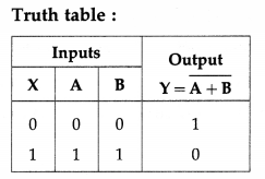
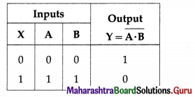
Which logic gate corresponds to the truth table
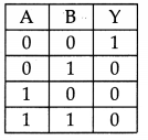
(A) AND
(B) NOR
(C) OR
(D) NAND
Answer:
(B) NOR
Question 24.
The logic gate which produces LOW output when any one of the input is HIGH and produces HIGH output only when all of its inputs are LOW is called
(A) an AND gate
(B) an OR gate
(C) a NOR gate
(D) a NAND gate.
Answer:
(C) a NOR gate
Question 25.
The Boolean expression for an Exclusive OR gate is
(A) A + B
(B) A ⊕ B
(C) \(\overline{\mathrm{A}+\mathrm{B}}\)
(D) A ∙ B
Answer:
(B) A ⊕ B